





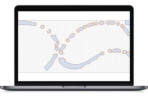







Asiga for Microfluidics: Turning Scientific Ideas into Functional Devices Faster

By Sergei Chapek, PhD
Microfluidics has become one of the most powerful engineering platforms for modern science. It allows researchers to manipulate fluids at the microliter and sub-microliter scale, create controlled chemical and biological environments, integrate multiple laboratory operations into compact devices, and accelerate experiments that would otherwise require complex glassware, expensive cleanroom processes, or long development cycles.
For many years, however, access to microfluidic device fabrication was limited. Traditional methods such as photolithography, soft lithography, glass micromachining, and silicon processing are extremely powerful, but they require infrastructure, trained personnel, and a relatively long design-to-device workflow. For a research group that needs to test a hypothesis quickly, this can become a bottleneck.
This is where high-resolution DLP 3D printing changes the logic of microfluidic development.
DLP printing does not simply offer “another way” to manufacture microfluidic chips. It gives scientists an agile fabrication tool that connects CAD design, experimental thinking, and functional device testing in a single workflow. In practical terms, it allows a researcher to move from an idea to a physical microfluidic prototype within hours or days, rather than weeks.
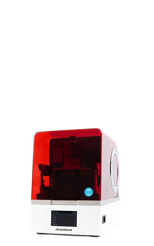
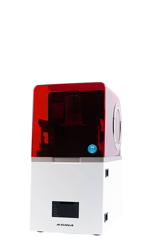
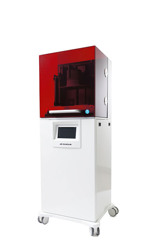
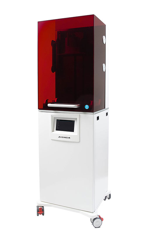
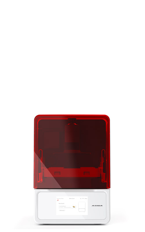
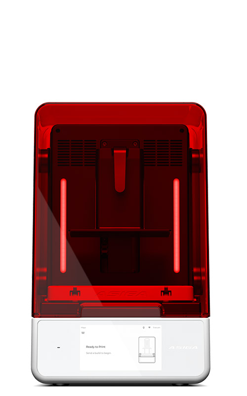
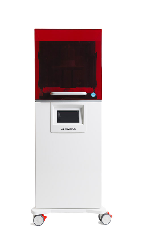
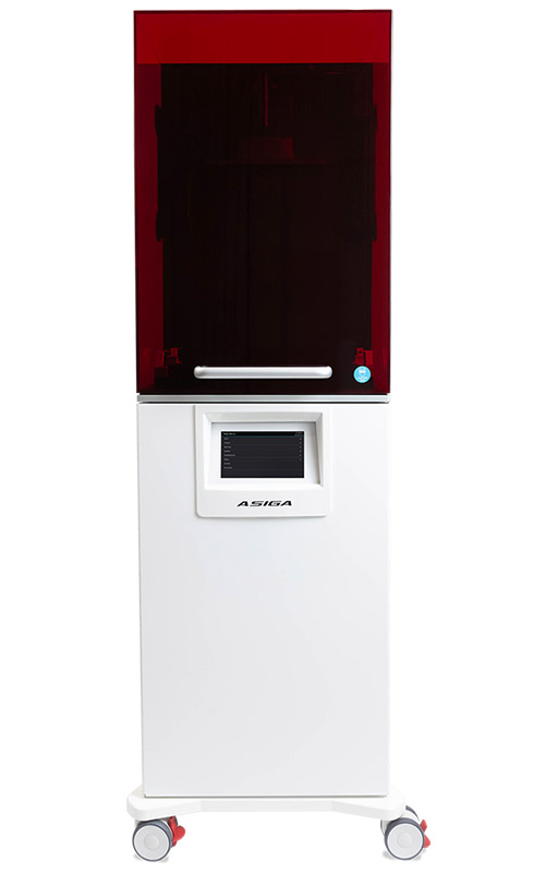
Asiga’s MAX X platform is particularly relevant for this field because the MAX X27 configuration provides a 27 µm pixel image, while the MAX X series also includes 35 µm and 43 µm configurations depending on the required balance between resolution and build area. Asiga also highlights 385 nm UV LED technology for fine detailing and processing of water-clear materials, both of which are important when working with small channels and optical access.
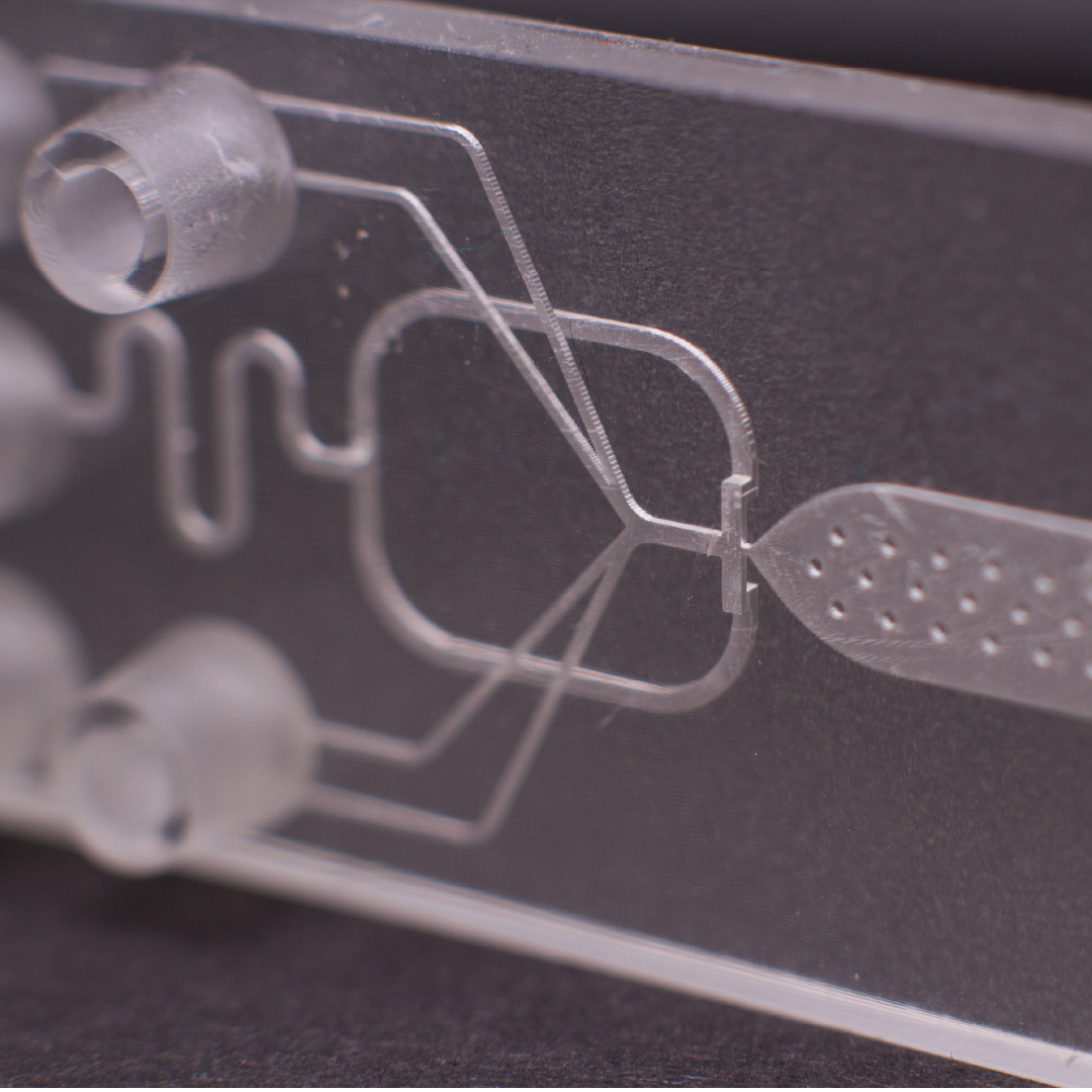
Microfluidics is no longer a niche technology used only in specialized labs. It is now relevant across several scientific and industrial domains. In flow chemistry, microfluidic reactors enable fast heat and mass transfer, precise residence time control, safer handling of reactive intermediates, and rapid screening of reaction conditions. In biomedical research, lab-on-a-chip systems can support cell culture, organ-on-chip studies, diagnostics, sample preparation, and controlled biological assays. Analytical chemistry also benefits, as microfluidic devices can integrate mixing, extraction, separation, dilution, reagent dosing, and detection in compact platforms. For materials science, controlled droplet generation, nanoparticle synthesis, emulsion formation, and polymerisation can all benefit from microfluidic environments. Finally, in education and rapid prototyping, universities can use 3D-printed microfluidic devices to teach students how fluidic systems work without requiring cleanroom infrastructure.
The core challenge is that microfluidic research is highly iterative. A channel geometry that looks promising in CAD may behave differently when real fluid enters the system. Bubbles, wetting, pressure drop, surface roughness, dead zones, particle clogging, and incomplete cleaning can all affect performance. Therefore, microfluidics needs a manufacturing method that supports fast design iteration, and DLP 3D printing provides exactly that.
In microfluidics, the most important question is not only whether we can print a small channel. The real question is whether we can print a functional fluidic system that can be connected, flushed, inspected, repeated, and used in a scientific experiment. DLP 3D printing is valuable because it allows researchers to integrate several functional elements directly into one monolithic device.
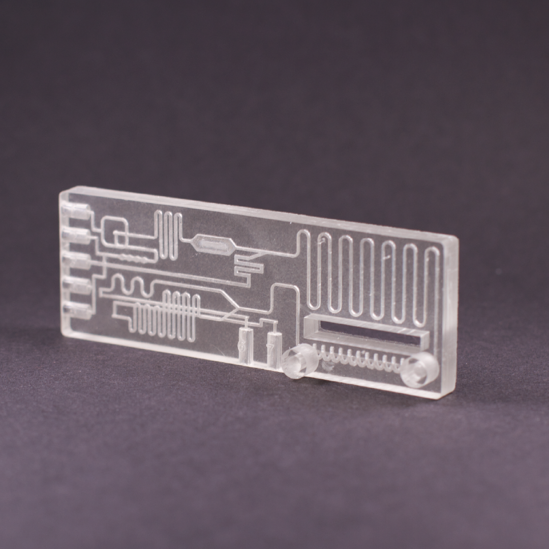
This integration includes microchannels and reaction zones, which can be designed as straight, serpentine, split-and-recombine, droplet-forming, or three-dimensional architectures. Passive mixing structures can also be integrated into the channel path without additional assembly. Furthermore, fluidic connectors like inlet and outlet ports can be designed directly into the device body, reducing assembly complexity. To support visual inspection, microscopy, or optical detection, transparent or semi-transparent resins can be used to create optical windows and observation zones, depending on material and post-processing quality. More complex lab-on-a-chip architectures—such as reservoirs, chambers, traps, and gradient generators—can be produced as single printed parts. Unlike planar soft lithography, three-dimensional channel routing allows channels to move in all three dimensions, enabling compact and non-planar fluidic layouts. This three-dimensional freedom is one of the most important advantages of additive manufacturing for microfluidics, allowing researchers to stop thinking only in layers and begin designing true volumetric fluidic architecture.
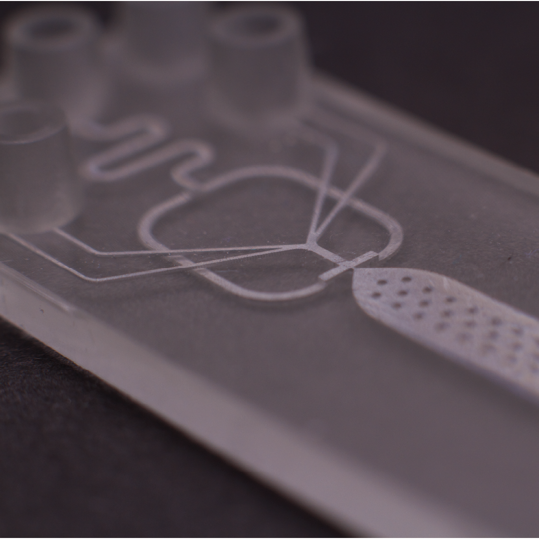
A common mistake is to assume that if a 100 µm channel is drawn in CAD, the printer will automatically create a clean 100 µm channel. In reality, microfluidic DLP printing is governed by the interaction of several factors. First, the pixel size and projected image geometry define the basic projected image unit. For example, with a 27 µm pixel image, a nominal 100 µm feature is represented by only a small number of pixels, meaning geometry should be designed with the pixel grid in mind, not only with ideal CAD dimensions. Second, the exposure dose must be carefully balanced; overexposure can cause channel narrowing or blockage because polymerisation extends beyond the nominal projected boundary, while underexposure can lead to weak walls, incomplete curing, or dimensional instability. Resin optical behavior, including resin absorption, scattering, pigment concentration, and photoinitiator chemistry, also strongly influences cure depth and lateral curing. Additionally, layer thickness affects vertical resolution, internal surface quality, exposure strategy, and the ability to form enclosed channels. The channel orientation relative to the build platform further affects resin drainage, optical penetration, layer formation, and cleaning efficiency. Finally, post-processing steps like washing, flushing, drying, and final curing are not secondary operations; in microfluidics, post-processing often determines whether the device works or fails. This is why microfluidic 3D printing should be treated as a complete process chain spanning design, slicing, exposure, printing, cleaning, curing, and testing, as the real result comes from controlling the full process rather than just relying on the printer.
When designing microfluidic devices for DLP printing, I recommend thinking in terms of manufacturability from the very first sketch. A good microfluidic CAD model is not only a beautiful channel network; it is a device that can be printed, cleaned, connected, and used. Several practical design principles are especially important.
To start, you should avoid treating the minimum printable feature as the working design limit. Even if very small features are technically possible, reliable microfluidics often requires a safety margin because a channel that prints once under ideal conditions may not be suitable for routine scientific work, and repeatability is more valuable than a single impressive demonstration. You must also design channels for cleaning, not only for flow. Uncured resin must be removed from internal channels, and because long, narrow, blind, or highly branched channels can be difficult to clean, the design should support direct flushing from inlet to outlet wherever possible. Additionally, it is wise to use test coupons before printing complex devices. Before printing a full microfluidic chip, it is useful to print a small test structure with channel sizes, orientations, and geometries similar to the final device to reduce material waste and gain fast feedback on exposure and the cleaning strategy. It is also important to think about connector integration early. Many microfluidic prototypes fail not because of the internal channel, but because of leakage, poor tubing connection, or fragile ports, meaning threaded ports, press-fit interfaces, ferrule-based connections, or custom adapters should be considered at the CAD stage. Lastly, you should separate optical, chemical, and mechanical requirements. A resin that gives excellent optical clarity may not be optimal for chemical resistance, and a mechanically strong resin may not be ideal for small transparent channels, so material selection must follow the experiment rather than just the printability requirement.
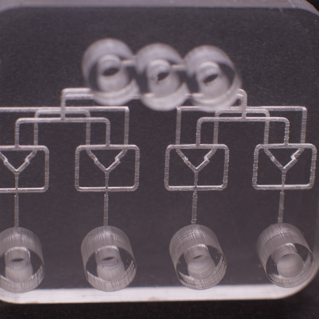
Materials are central to microfluidic DLP printing. For scientific applications, the resin must be evaluated not only by its ability to print fine features, but also by its behavior in the actual experiment. Important material properties include viscosity, as lower viscosity generally helps with resin drainage and channel cleaning, especially in enclosed geometries. Optical transparency is also vital for visual inspection, microscopy, absorbance measurements, fluorescence observation, or image-based analysis. Chemical compatibility must be addressed since the device may be exposed to solvents, acids, bases, monomers, biological media, oils, surfactants, or reactive intermediates. Surface properties, including hydrophilicity, hydrophobicity, surface energy, and protein adsorption, can strongly influence fluid behavior. For biological applications, biocompatibility traits like cytotoxicity and leachable components must be carefully considered. Mechanical stability is required so that thin walls, ports, and pressure-loaded channels remain stable during use. Finally, post-curing behavior must be monitored because shrinkage, brittleness, optical yellowing, and final conversion after curing can affect device performance. The future of 3D-printed microfluidics will not be defined only by printer resolution, but also by the development of purpose-built resins for microfluidic science that are transparent, low-viscosity, chemically stable, biologically compatible, and surface-tunable.
DLP 3D printing can support many types of microfluidic devices. Some of the most promising include flow chemistry microreactors, where small channels enable precise control of residence time, temperature, mixing, and reagent contact, allowing researchers to rapidly test channel geometries for synthesis, crystallisation, extraction, or multiphase reactions. Droplet microfluidics is another key area where T-junctions, flow-focusing geometries, and step emulsification structures can be prototyped for droplet generation, encapsulation, emulsion production, and screening. Gradient generators can also be created, utilising networks of splitting and recombination channels to form concentration gradients for chemical, biological, or materials experiments. For biological studies, cell culture devices with 3D-printed chambers, perfusion channels, and scaffold-like environments can be produced when suitable materials and post-processing protocols are used. Analytical devices can integrate sample preparation, reagent mixing, optical detection windows, and compact fluidic routing into microfluidic chips. Finally, educational microfluidics benefits significantly, as DLP printing allows students and early-stage researchers to design, print, and test devices quickly, making microfluidics more accessible as a teaching platform.
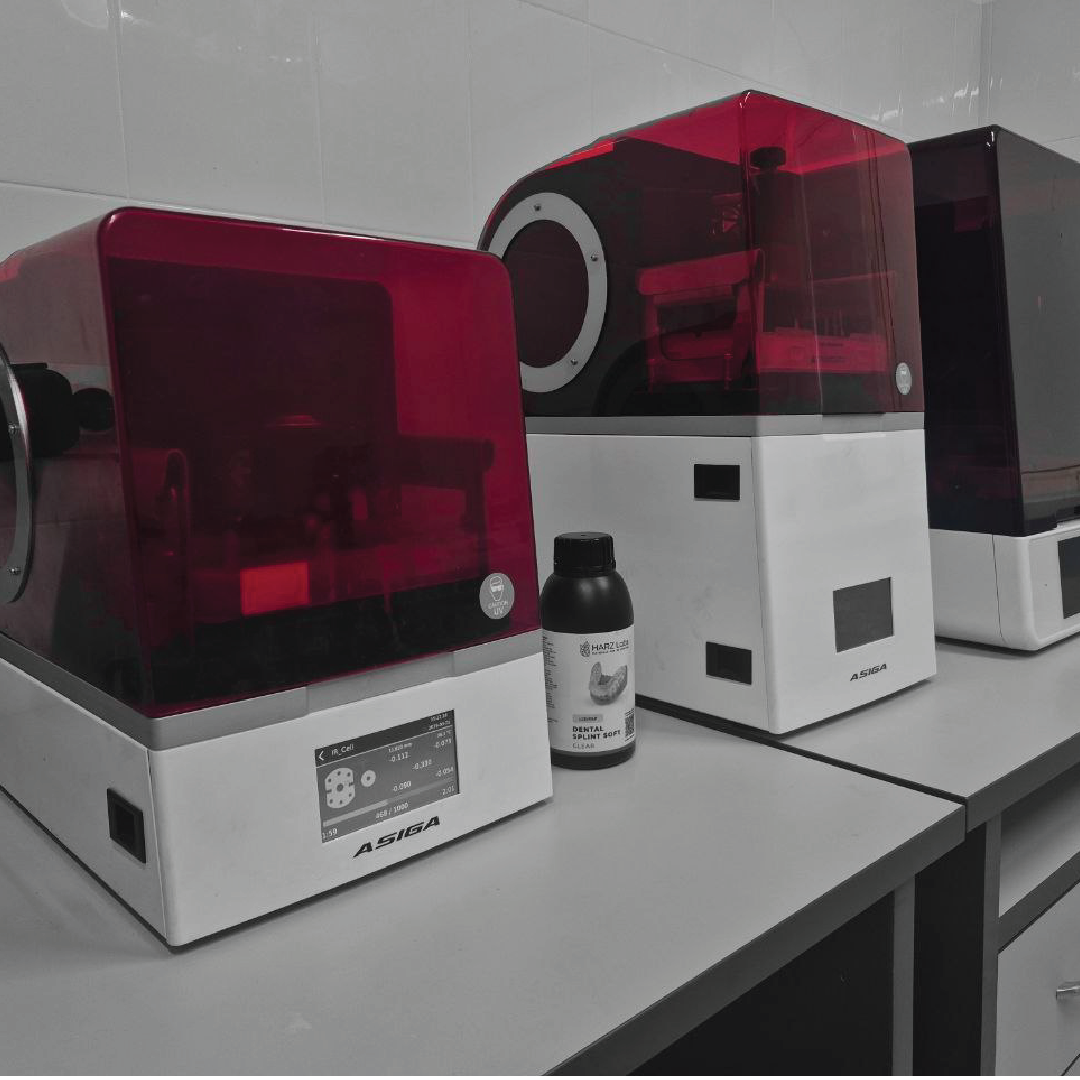
For scientific laboratories, the key benefit of DLP printing is not only precision, but iteration speed. A research group can design a device in CAD, print several variants overnight, test flow behaviour the next day, modify the geometry, and repeat the cycle. This ability changes the culture of microfluidic development. Instead of waiting for external fabrication or cleanroom access, scientists can build experimental hardware directly inside the lab. For early-stage research, this is strategically important because many scientific ideas are uncertain at the beginning. Researchers need to explore geometry, material, flow rate, pressure, mixing, and surface behaviour, and DLP printing supports this exploration because it lowers the cost and time of failure, making microfluidic R&D far more agile.
DLP 3D printing is powerful, but it is not magic. For serious microfluidic work, limitations must be understood clearly. First, internal channels can be difficult to clean; the smaller and longer the channel, the more difficult it becomes to remove uncured resin, meaning the cleaning strategy must be part of the design. Second, optical clarity depends on more than resin transparency, as layer lines, surface roughness, post-curing, polishing, wall thickness, and resin formulation all influence final optical quality. Third, chemical compatibility must be validated, since not all photopolymer resins tolerate aggressive solvents or reactive chemicals, and swelling, cracking, softening, or leaching may occur. Fourth, surface chemistry may need modification, particularly for applications involving droplets, cells, proteins, or capillary-driven flow where specific surface treatments are required. Finally, dimensional accuracy is highly process-dependent, as exposure settings, resin temperature, part orientation, support strategy, and post-curing can all influence final channel dimensions. The correct mindset is to see DLP printing as an engineering platform that requires calibration, validation, and process discipline, which allows it to become an extremely effective tool for scientific device development.
For laboratories starting with DLP microfluidics, I recommend following a highly structured workflow. You must define the experiment first by identifying the fluid, flow rate, pressure range, optical requirements, chemical exposure, and cleaning method. Next, select the resin based on the application, making sure not to select the material only because it prints well, but because it supports the actual experiment. From there, design test structures to print simple channel arrays with different widths, heights, orientations, and lengths. You can then optimise exposure and layer settings to evaluate whether the channels remain open, dimensions are stable, and walls are sufficiently strong. Following this, develop a cleaning protocol to test flushing solvents, pressure-assisted cleaning, drying, and the post-curing sequence. Once this is established, validate fluidic performance by checking for leakage, pressure resistance, bubble formation, wetting behaviour, and flow repeatability. Only after completing these steps should you print the full device, ensuring that complex devices are built strictly on validated process knowledge. This approach saves time and prevents the most common failure mode, which is printing a sophisticated device before the process window is thoroughly understood.
The democratisation of microfluidic fabrication is a major opportunity for science. DLP 3D printing allows smaller laboratories, universities, startups, and interdisciplinary teams to enter the field of microfluidics without immediately investing in cleanroom infrastructure, providing chemists, biologists, materials scientists, and engineers a shared tool for building experimental systems. This is especially important for translational research, where many scientific discoveries fail to move forward because the physical experimental platform is too difficult to fabricate or modify. With high-resolution DLP printing, the device itself becomes part of the research process, allowing scientists to ask crucial questions regarding changes to mixer geometry, reducing dead volume, integrating reaction chambers with optical windows, or direct comparisons of several printed channel architectures. Researchers can even build a custom device for one specific experiment, providing the exact flexibility that modern research needs.
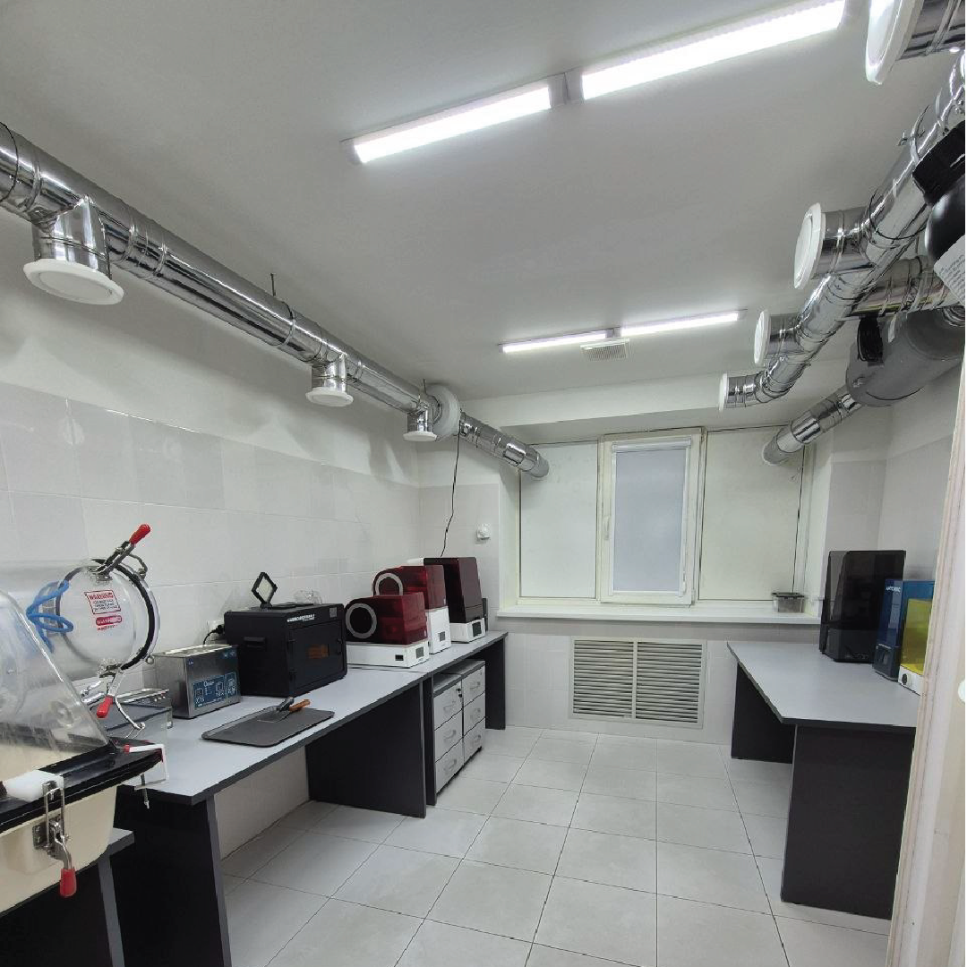
The next stage of DLP microfluidics will go beyond simple chips, moving toward more integrated systems. We will see setups combining microchannels, optical detection zones, embedded functional surfaces, modular connectors, reaction chambers, cell culture regions, droplet generators, thermal control elements, sensor integration, and application-specific resin chemistry. In the long term, DLP printing can help transform microfluidics from a specialised fabrication discipline into a standard scientific tool, similar to how desktop 3D printing changed mechanical prototyping. For this to happen, the community needs not only better printers, but also better design rules, validated materials, open workflows, and shared experimental data.
About the Author
Sergei Chapek is a distinguished expert in additive manufacturing and 3D printed microfluidics, leveraging an extensive background in law and international relations to drive innovation in technology. He graduated from the Law Faculty at Southern Federal University with a degree in International Law in 2007, laying the groundwork for his career in navigating complex legal frameworks and fostering international cooperation.
From 2009 to 2018, Sergei held the position of Commercial Director, where he oversaw international collaborations in several companies. This period honed his skills in strategic negotiation and partnership development, crucial for operating in a globalized economy.
In 2019, seeking to blend his legal expertise with emerging technological advancements, Sergei graduated from the Diplomatic Academy of the Ministry of Foreign Affairs of the Russian Federation. He received a second degree in International Relations, and his master’s thesis focused on “International Technology Transfer and its Mechanisms Regulation in Modern International Relations.” This work marked a pivotal transition from humanitarian studies to the natural sciences and engineering, igniting his passion for technology.
The fascinating world of additive manufacturing drew Sergei’s attention, leading to his appointment in 2018 to head a laboratory at a Don State Technical University dedicated to adapting 3D printing technology for medical applications including a 3D bioprinting technology. This experience solidified his enthusiasm for 3D printing and opened new avenues for research and development.
Currently, Sergei holds a position as a head of the Additive Technologies Department at the Smart Materials Research Institute. Under his leadership, the department has become a cornerstone of the institute’s growth, particularly in the innovative 3D printing of microfluidic devices. In 2021, the laboratory acquired its first Asiga MAX UV printer, now they have a pool of Asiga printers to meet the increasing demand for 3D printed microfluidics and micro mechatronics production.
Since 2022, Sergei has been recognized as a Key Opinion Leader (KOL) for Asiga, further solidifying his position at the forefront of the field. His journey from law to technology exemplifies the transformative potential of interdisciplinary collaboration and innovation, establishing him as a pivotal figure in advancing additive manufacturing and its applications in modern science.
Share: